The Bare Board Fabrication Process Revealed
15 to 30 discrete steps are required to build your unique bare circuit board. The following will provide the Newbie Buyer or Program Manager some vocabulary and insight into this complex and time proven manufacturing process.
Overview of double sided printed circuit boards using the panel plating procedure
CAM ( Computer Aided Manufacturing )
 The purpose of the CAM process is to check and prepare your electronic CAD files. This is the electronic interface between your process and ours. We look for obvious errors and will call you if something looks out of place. We accept files in Gerber format of 274X (preferred) or 274D. It is critical that your design fit our process and receives a final review before committing to the factory floor.
Film Generation
 The output from the CAM process is the film used for making your images. This can be either a negative or a positive depending upon need. Circuit creation is basically a contact printing process. Our high resolution photoplotter makes the silver transparencies for contact printing your circuit patterns, solder mask openings, and silk screen legends. These films are used to transfer the image onto the fresh copper panels in the case of circuit creation ( Copper Laminate ), provide the openings in the soldermask for applying a final conductive finish, and imaging high resolution white legend on your final product.
Copper Laminate
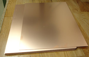
Core building block of your board consisting of rolled or electrodeposited copper on both sides of a woven glass fiber core.
Drilling
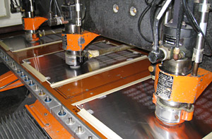
High speed computer controlled drilling machines use x-y coordinate data from your CAD files to precisely drill the copper laminate. Accuracy is to .001″
Electro Plating

Copper is required inside the new holes to connect the top, inner cores, and the bottom surface electrically. Typically we need to add some copper thickness to the top and bottom surface of the panels as well.
The electroplate process is an electrified bath of copper sulfate and chemical brighteners. Copper bars or baskets of copper balls are extended into the bath. The boards ( panels ) are also extended into the bath. The panels are then connected to one side of the circuit and the copper bars to the other side. The resulting flow of electrical energy boils off copper molecules from the bars which are attracted to the copper panels. All exposed surfaces which are metallic will attract this bombardment of copper. Typically we add from .001” to ..0025” of copper to the holes and exposed surfaces.
Imaging
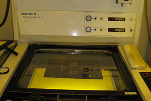
Special etch resistant film ( Resist ) is applied to the drilled and plated copper panels. Your silver film is then precisely aligned ( Registered ) onto the panels and exposed under 5kw mercury vapor lamps. This transfers the image onto the panel (Contact Printing.) Once exposed, the panels are washed in a developing bath to remove the non-exposed areas and leaving hardened resist over the desired circuit traces.
Etching
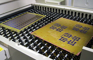
Once the critical circuit paths are covered with the hardened resist, the panel is chemically milled ( copper etching ) to remove unwanted copper. This is a very precise process and the result yields your exact circuit pattern.
Soldermask
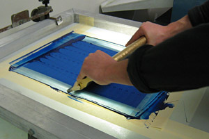
Application of a durable epoxy coating ( green normally ) which covers the circuit traces and leaves openings where solder pads are required. The process involves 3 major steps: (1 ) flood the panel with a thin even coating of photo imagable epoxy, (2) contact print using a soldermask film which defines the openings, (3) develop ( wash with pressure sprayers in a solution of potassium and water). The panel then gets a long bake in a hot oven. Your panel is now ready for final finishing with solder, gold , Tin, or Silver.
Final Surface Finishing

Hot air solder leveling ( HASL ) is the most common final finish. This can be done with either tin/lead or lead free (tin/copper alloy )solder. To apply the solder, the boards are cleaned, flux is applied, then dipped in a bath of molten solder. As the board is extracted from the solder powerful jets of air level the solder before it hardens. Done correctly, this leaves a flat smooth surface. It is fast and inexpensive.
Also common is nickel / gold ( ENIG ) for lead free applications and high performance circuits. Less common but growing in popularity is Immersion Tin as a lead free alternative. Pictured on the right is a ENIG processing line. The advantage of these final finishes for fine surface mount assemblies is the natural “flatness” of the final surface. Flat surfaces mean small parts mount correctly.
Legend
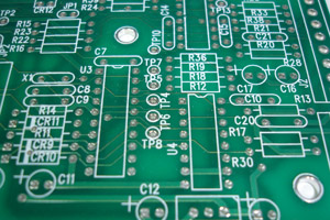
The application of the identifying information on the top and bottom of the board. This information assists the assemblers in component placement, technicians in repair, and provides a means of adding other circuit card information for the user. Old school is screen printing this information. Current technology uses photoimagable ink and contact printing for crisp lettering in extremely tight spaces.
Rout to Shape
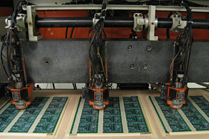
All individual boards are imaged on a larger master panel. After the board is complete it is cut out (routed) to the precise shape you require. This is done on the same or similar equipment as the drilling and from your original CAD files data.
Test
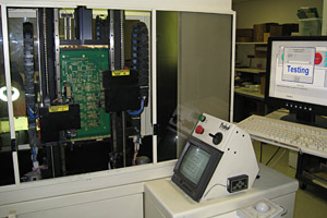
From the original CAD files we extract a net list ( list of all circuit connections by x-y location ). These are the instructions for the automated point to point circuit testing. We test for both continuity and discontinuity. All circuits should be checked to assure a good board going into assembly. We use both flying probe for small jobs and a bed of nails contact method for higher volume boards. Pictured at right is a flying probe tester. The boards are mounted vertically and 4 very fine probe tips dance around the board front and back measuring continuity and discontinuity by making contact with all of the pads. An easy test to determine if your board was actually tested in this manner is to look for a small indentation on the pads.
Inspection
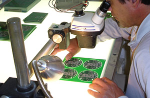
A final visual check for cosmetic flaws is always performed under magnification or microscope to assure a perfect product out the door.
This a brief explanation of the processes for a Double Sided board. For multilayer panels we repeat each step for each pair of layers plus another dozen steps…
Total Manufacturing Steps
- Two Sided Board > 15
- Multilayer Board > 25
The Bare Circuit Card – The most custom part of your hardware design
